


1. Product Overview
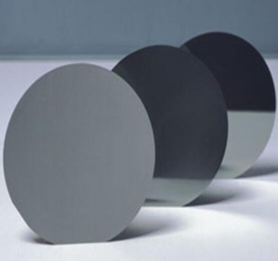
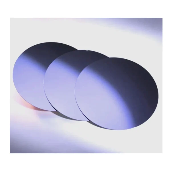
Monocrystalline Silicon Wafer is a high-purity semiconductor-grade silicon substrate manufactured from a single-crystal silicon structure, providing excellent electrical and structural uniformity. It is primarily used in the production of high-efficiency photovoltaic cells, semiconductor devices, integrated circuits, and advanced electronic components. Its superior crystal quality, consistent performance, and excellent carrier mobility support higher device efficiency and reliable large-scale manufacturing. As a critical input for the global semiconductor and renewable-energy industries, monocrystalline silicon wafers are strategically important for advanced electronics and next-generation solar technologies.
2. Key Specifications & Technical Characteristics
- Material: Monocrystalline silicon (single-crystal silicon)
- Chemical Composition: Silicon (Si), with controlled trace dopants according to application requirements
- Purity: Typically high-purity silicon; grade and purity available according to specified photovoltaic or semiconductor requirements
- Crystal Structure: Single-crystal monocrystalline structure
- Appearance: Flat, smooth silicon wafer; typically silver-grey to dark-grey depending on surface treatment
- Wafer Type: P-type or N-type available according to application
- Surface Finish: Polished, textured, or application-specific surface treatment
- Dimensions: Available in various industry-standard wafer sizes and thicknesses according to buyer specification
- Electrical Characteristics: Controlled resistivity and doping levels available to meet application requirements
- Packaging: Protective wafer boxes, trays, cartons, or customized export packaging
- Shelf Life: Long-term storage when kept sealed in clean, dry, contamination-controlled conditions
- Customization: Diameter, thickness, doping, resistivity, surface treatment, and other technical parameters available according to specification
3. Core Industrial Applications
- Solar Photovoltaics: Used as the primary substrate for manufacturing high-efficiency monocrystalline solar cells and photovoltaic modules.
- Semiconductor Manufacturing: Serves as a foundational substrate for integrated circuits, microelectronics, sensors, and other semiconductor devices.
- Electronics Industry: Used in the fabrication of advanced electronic and power-management components requiring precise electrical characteristics.
- Research & Advanced Technology: Supports laboratories, R&D facilities, and specialized applications requiring controlled single-crystal silicon substrates.
- Why It Performs Better: The uniform single-crystal structure delivers consistent electrical properties, high carrier mobility, and excellent process control, supporting efficient manufacturing and reliable device performance compared with lower-quality or less uniform silicon substrates.
4. Competitive Advantages
- Quality Consistency: Controlled crystal structure, dimensions, surface quality, and electrical characteristics support repeatable industrial processing.
- Supply Reliability: Suitable for structured B2B procurement and recurring bulk requirements, helping buyers maintain production continuity.
- Logistics Capability: Export-oriented packaging and bulk shipment solutions support international industrial supply chains.
- Price Competitiveness: Bulk sourcing and optimized procurement volumes can provide commercially competitive pricing for large-scale projects.
- Sustainability: Enables high-efficiency photovoltaic technologies that contribute to renewable-energy generation and the transition toward lower-carbon power systems.
- Technical Documentation: Product specifications, quality documentation, inspection records, and relevant certificates can be provided according to order and application requirements.
- Strategic Sourcing Value: A scalable supply option for manufacturers, distributors, solar developers, and technology companies seeking consistent silicon wafer supply for high-volume operations.
5. Commercial & Supply Information
- Minimum Order Quantity (MOQ): BULK – 20 MT
- Loading Capacity: Up to 20 MT per container, subject to wafer specifications, packaging configuration, and applicable container weight limits
- Packaging: Export-grade protective packaging designed to minimize handling and transportation risks
- Supply: Bulk and recurring supply programs available according to buyer requirements


Reviews
There are no reviews yet.